Design Linked Incentive Scheme Catalyses India’s Semiconductor Design Ecosystem
New Delhi, January 5: The Design Linked Incentive (DLI) scheme, a flagship initiative under the Semicon India Programme, is rapidly emerging as a cornerstone of India’s strategy to build a
Launched by the Ministry of Electronics and Information Technology (MeitY), the scheme is strengthening India’s fabless chip design capabilities—widely regarded as the most value-intensive segment of the global semiconductor value chain.
New Delhi, January 5: The Design Linked Incentive (DLI) scheme, a flagship initiative under the Semicon India Programme, is rapidly emerging as a cornerstone of India’s strategy to build a self-reliant and globally competitive semiconductor design ecosystem. Launched by the Ministry of Electronics and Information Technology (MeitY), the scheme is strengthening India’s fabless chip design capabilities—widely regarded as the most value-intensive segment of the global semiconductor value chain.
According to official data, semiconductor chip design contributes up to 50 percent of total value addition, accounts for 20–50 percent of the bill of materials cost, and drives 30–35 percent of global semiconductor revenues through the fabless model. Recognising this strategic leverage, the DLI Scheme aims to reduce India’s dependence on imported semiconductor intellectual property while fostering indigenous innovation across critical sectors.
Strong Momentum and Measurable Outcomes
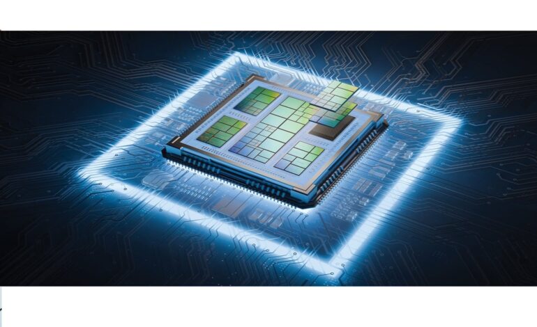
Since its launch in December 2021, the DLI Scheme has supported 24 chip design projects targeting strategic applications such as video surveillance, drone detection, energy metering, microprocessors, satellite communications, broadband and IoT systems-on-chip. These projects have already delivered tangible outcomes, including 16 design tape-outs, six fabricated ASIC chips, ten patents, and engagement of over 1,000 specialised engineers.
The scheme has also succeeded in leveraging more than three times private investment, signalling growing confidence among industry players in India’s semiconductor design potential.
Financial Incentives and Infrastructure Support
Under the DLI framework, eligible startups and MSMEs receive reimbursement of up to 50 percent of eligible design expenditure, capped at ₹15 crore per project, along with deployment-linked incentives of 4–6 percent of net sales turnover for five years. The incentive for deployment is capped at ₹30 crore per application.
To complement financial support, MeitY—through C-DAC—has established the ChipIN Centre, providing shared national design infrastructure. This includes access to a National EDA Tool Grid, IP core repositories, multi-project wafer (MPW) prototyping support and post-silicon validation facilities.
Notably, the EDA Grid has recorded over 5.4 million cumulative usage hours, making it the world’s largest centrally accessed chip design infrastructure. Nearly 95 startups and over 300 academic institutions are currently benefiting from this ecosystem.
Enabling Strategic Autonomy
Officials highlight that without strong fabless capabilities, even countries with advanced electronics manufacturing remain dependent on imported core technologies. By focusing on chip design and IP ownership, the DLI Scheme positions India to retain high-value intellectual property, enhance supply-chain resilience, and attract downstream manufacturing investments.
The programme also aligns with complementary initiatives such as the Chips to Startup (C2S) Programme, which aims to create 85,000 industry-ready semiconductor professionals, and the Microprocessor Development Programme, which has delivered indigenous processor families including VEGA, SHAKTI and AJIT.
Emerging Success Stories
Several DLI-supported companies have already gained global traction. These include startups developing indigenous AI-enabled surveillance SoCs, motor-control chips for consumer and automotive applications, RISC-V microprocessor IPs, broadband network processors and radar-on-chip solutions for defence and smart infrastructure.
These success stories underline how the DLI Scheme is converting research-grade innovation into silicon-proven, market-ready products, marking a decisive shift from experimentation to productisation.
Looking Ahead
As India’s semiconductor ecosystem enters the next phase, DLI-supported firms are now moving towards volume manufacturing, system integration and global market deployment. Policymakers say this transition will reinforce India’s strategic autonomy in critical technologies while positioning the country as a credible global hub for semiconductor design.
With rising global demand and increasingly fragile supply chains, the Design Linked Incentive Scheme is widely viewed as a timely and transformative intervention—anchoring India firmly in the most strategic layer of the semiconductor value chain.