India’s First 3D Semiconductor Packaging Unit Breaks Ground in Odisha; ₹2000 Cr Boost to AI, 5G and Defence Tech
The project, led by 3D Glass Solutions through its Indian arm, marks a significant milestone in strengthening India’s domestic semiconductor ecosystem and advancing the vision of Atmanirbhar Bharat. Bhubaneswar: In
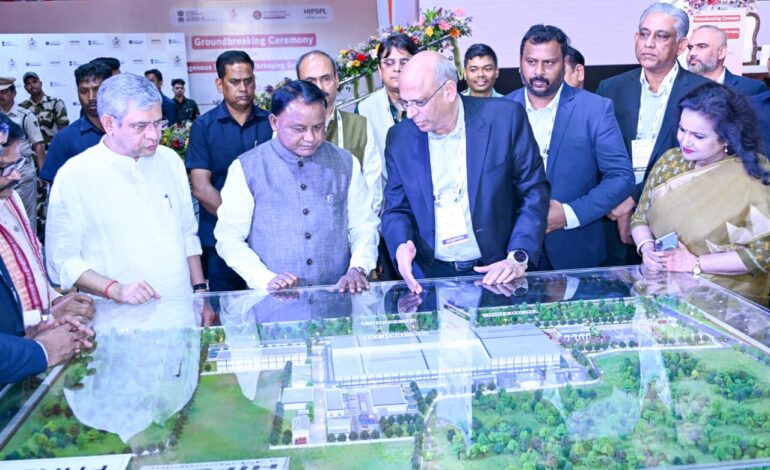
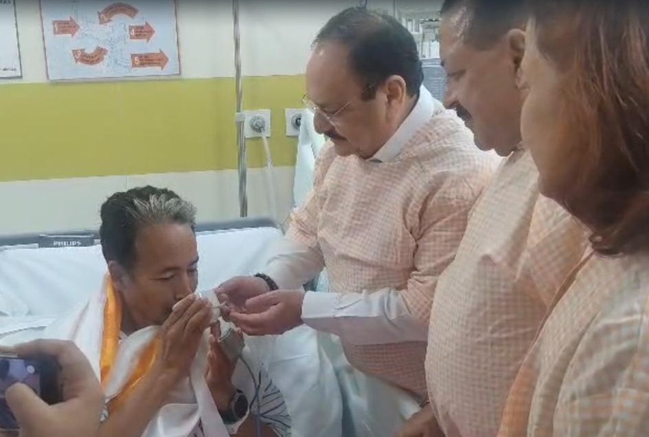
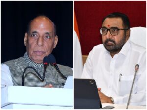
Odisha Chief Minister Mohan Charan Majhi, Union Minister for Electronics and IT Ashwini Vaishnaw during the foundation stone laying ceremony for the country’s first advanced 3D chip packaging unit at Info Valley, Bhubaneswar, on Sunday.
The project, led by 3D Glass Solutions through its Indian arm, marks a significant milestone in strengthening India’s domestic semiconductor ecosystem and advancing the vision of Atmanirbhar Bharat.
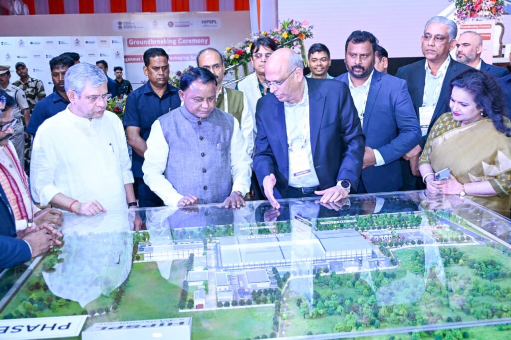
Bhubaneswar: In a major leap for India’s semiconductor ambitions, the foundation stone for the country’s first advanced 3D chip packaging unit was laid at Info Valley in Bhubaneswar, positioning Odisha as a rising hub for high-end electronics manufacturing.
The project, led by 3D Glass Solutions through its Indian arm, marks a significant milestone in strengthening India’s domestic semiconductor ecosystem and advancing the vision of Atmanirbhar Bharat.
Speaking at the event, Chief Minister Mohan Charan Majhi described the initiative as a historic moment for both the state and the nation. He highlighted that this is the first time such advanced 3D semiconductor packaging technology is being established in India, placing Odisha on the global technology map.
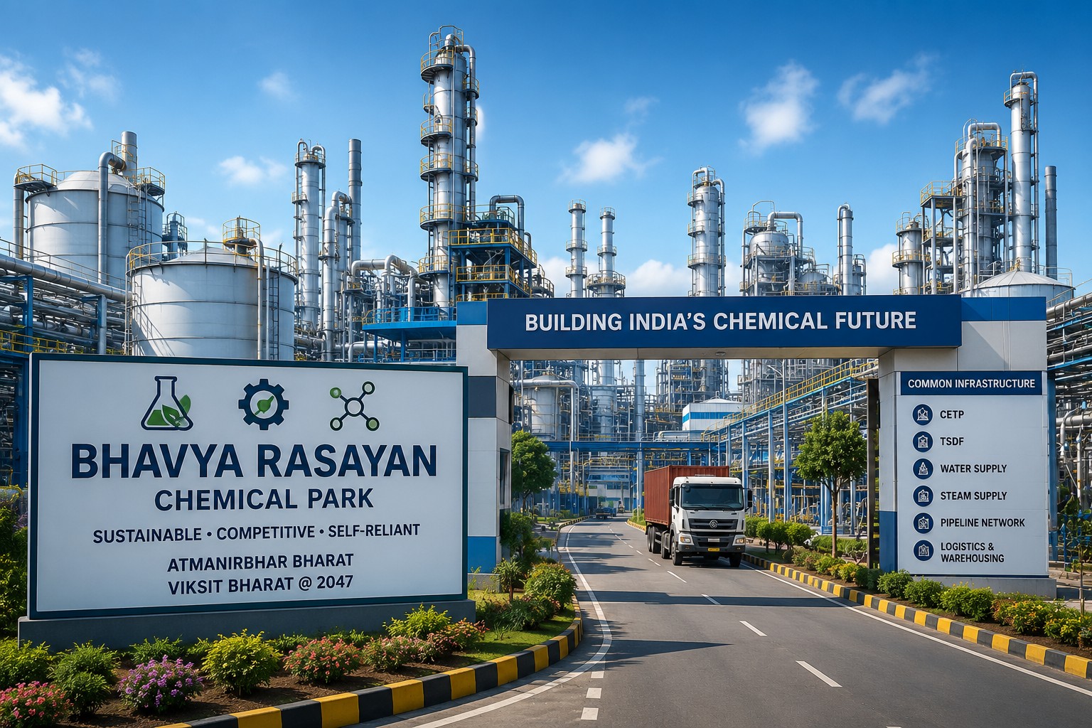
The facility, coming up in Khordha district, involves an investment of nearly ₹2,000 crore and is expected to produce 70,000 glass panels annually, along with 50 million assembled units and 13,000 advanced 3D heterogeneous integration modules.
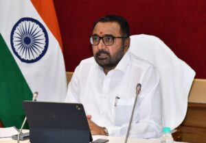
Union Minister for Electronics and IT Ashwini Vaishnaw said the project reflects the rapid progress of India’s semiconductor sector under the leadership of Narendra Modi. He noted that India has already emerged as the world’s second-largest mobile phone manufacturer and became the leading exporter of mobile phones in 2025.
“Odisha, traditionally known for minerals and metals, is now steadily building capabilities in electronics, IT and semiconductors,” Vaishnaw said, adding that the project will significantly strengthen India’s semiconductor value chain.
The facility will cater to high-growth sectors including artificial intelligence, machine learning, 5G/6G communications, defence electronics, aerospace, automotive radar and photonics. Commercial production is expected to begin by August 2028, with full-scale operations targeted by 2030.
Officials said Odisha is currently the only state hosting both India’s first compound semiconductor fabrication unit and this advanced 3D packaging facility, reinforcing its position as a fast-emerging semiconductor hub.
The project is also expected to generate significant employment opportunities for engineering graduates, diploma holders and ITI students, supporting the state’s transition towards a technology-driven economy.
With additional semiconductor proposals in the pipeline and ongoing discussions with global players such as Intel, the development signals growing investor confidence in India’s electronics manufacturing ecosystem.
About the Project
The Heterogeneous Integration Packaging Solutions facility is a greenfield, vertically integrated advanced packaging and embedded glass substrate ATMP unit being developed with central and state support. It aims to deliver next-generation semiconductor solutions critical for emerging digital and defence technologies.