India Launches Indigenous Silicon Photonics Tools; IIT Madras Drives Strategic Semiconductor Capability
The PDK includes a library of over 50 verified components, enabling industries, startups, academic institutions and defence R&D organisations to design advanced photonic integrated circuits. Chennai: India has taken a
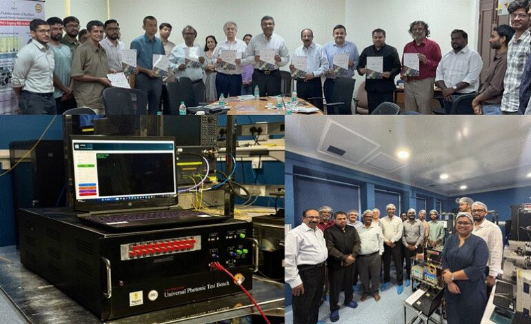
The Silicon Photonics Process Design Kit (PDK) and Universal Programmable Photonic Integrated Circuit (PPIC) Test Engine were launched by S. Krishnan, secretary, ministry of electronics and information technology, in Chennai on Friday.
The PDK includes a library of over 50 verified components, enabling industries, startups, academic institutions and defence R&D organisations to design advanced photonic integrated circuits.
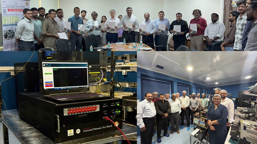
Chennai: India has taken a significant step towards semiconductor self-reliance with the launch of indigenous silicon photonics technology solutions developed at Indian Institute of Technology Madras, aimed at strengthening the country’s capabilities in next-generation chip design and manufacturing.
The solutions – a Silicon Photonics Process Design Kit (PDK) and a Universal Programmable Photonic Integrated Circuit (PPIC) Test Engine – were launched by S. Krishnan, Secretary, Ministry of Electronics and Information Technology (MeitY), marking a major milestone in India’s push for technology sovereignty in the photonics domain.
According to an official note, the PDK includes a library of over 50 verified components, enabling industries, startups, academic institutions and defence R&D organisations to design advanced photonic integrated circuits. The PPIC Test Engine, meanwhile, serves as an automated platform for characterisation of photonic and optoelectronic modules across applications.
The initiative has been developed under the MeitY-supported Centre of Excellence for Silicon Photonics (CoE-CPPICS) at IIT Madras and is expected to function as a shared national facility for India’s photonics research ecosystem.
Krishnan said the development positions India at par with global advances in silicon photonics and emphasised the need to complement this progress with the establishment of a dedicated silicon photonics fabrication facility under the India Semiconductor Mission.
Amitesh Sinha, additional secretary, MeitY and CEO of the India Semiconductor Mission, noted that the technology has applications across both classical and quantum domains, and could be supported further under the proposed ISM 2.0 framework to enable product development and commercialisation.
The centre is expected to begin multi-project wafer (MPW) fabrication runs from the third quarter of the current financial year, while offering integrated capabilities in testing, packaging and module characterisation.
Developed under a product research, development and manufacturing model, the initiative leverages global partnerships, including SilTerra Malaysia as foundry partner and izmo Microsystems, Bengaluru, for photonic IC packaging.
The launch underscores India’s broader push to build domestic capabilities in advanced semiconductor technologies, including silicon photonics, which are critical for high-speed data communication, AI infrastructure and quantum computing systems.