SEMICON India 2026 moves from semiconductor ambition to execution at scale
Day 2 of SEMICON India 2026 highlighted India’s expanding semiconductor ecosystem, with ISM 2.0, chip design, advanced packaging, resilient supply chains, global partnerships and talent development at the centre.
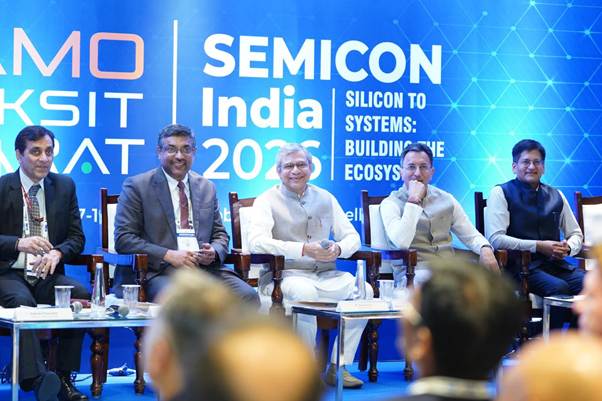
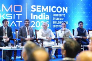
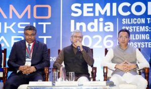
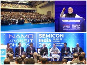
Held at Yashobhoomi in New Delhi, Day 2 brought together policymakers, global semiconductor companies, Indian industry, researchers, startups, academia and students to examine how India can build an integrated and globally competitive “Silicon to Systems” ecosystem.

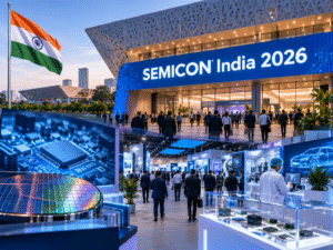
NEW DELHI: India’s semiconductor journey is moving from ambition to execution at scale, with the second day of SEMICON India 2026 highlighting advances across chip design, manufacturing, advanced packaging, materials, research, talent and international partnerships.
Held at Yashobhoomi in New Delhi, Day 2 brought together policymakers, global semiconductor companies, Indian industry, researchers, startups, academia and students to examine how India can build an integrated and globally competitive “Silicon to Systems” ecosystem. Around 16,000 participants attended the event during the day.
ISM 2.0 to expand the semiconductor ecosystem
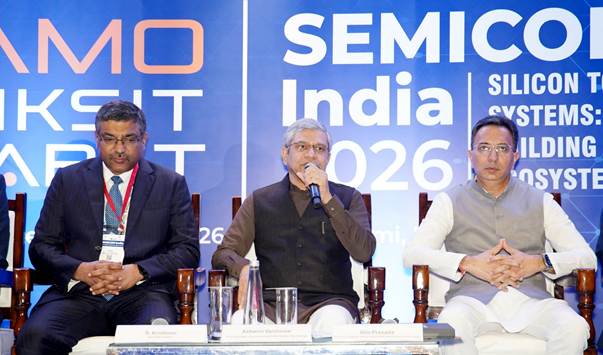
Union Minister for Electronics & Information Technology, Railways, and Information & Broadcasting Ashwini Vaishnaw said India’s semiconductor mission had moved from proving intent to executing projects at scale.
He said the second phase of the India Semiconductor Mission (ISM 2.0) would build on the foundation created under ISM 1.0 through six pillars — design; machines and materials; setting up more fabs; strengthening the ATMP/OSAT industry; research and development; and talent development.
According to Vaishnaw, ISM 1.0, originally conceived as a six-year programme, achieved its objectives in four years. He expressed confidence that ISM 2.0 would similarly progress ahead of schedule, supported by growing investor interest.
India targets 200 chip design companies
Chip design emerged as one of the areas where India already has a significant base of engineering and technology capabilities.
Vaishnaw estimated that at least 200 chip design companies could emerge under ISM 2.0, describing the development as a potential “game changer” for building home-grown semiconductor intellectual property.
More than 105 chip design startups have already gained access to advanced Electronic Design Automation tools, while 20 startups have secured venture capital funding. Around 70,000 chip-design engineers have been trained over the past four years against a target of 85,000.
The Minister also highlighted progress in manufacturing, noting that five of the 12 plants approved under ISM 1.0 have commenced commercial production. He emphasised that global competitiveness would depend not only on technological quality but also on competitive costs.
India’s growing reputation as a trusted country, along with its record in intellectual property protection, was also highlighted as an important factor in attracting semiconductor investments and technology partnerships.
From design services to a “Product Nation”
During his interaction with the media, Vaishnaw said the response to SEMICON India 2026 had been strong, with extensive business-to-business engagements and participation from major semiconductor economies.
The Country Roundtables, he said, demonstrated growing international interest in expanding engagement with India.
An important transition underway, according to the Minister, is India’s movement from a design-services model towards becoming a “Product Nation”, with Indian-designed chips increasingly finding their way into end products.
He also identified semiconductor machines and materials, specialised logistics, sustainability, water recycling and industry-ready talent as important components of the emerging ecosystem.
25 MoUs and strategic collaborations
Day 2 saw 25 MoUs, announcements and strategic collaborations involving Indian and global ecosystem partners.
The initiatives covered semiconductor materials, manufacturing, power electronics, advanced packaging, logistics, chip design and skilling.
The collaborations include efforts to localise critical materials, develop indigenous Silicon Carbide power technologies, expand access to semiconductor design tools, promote deep-tech investment, strengthen specialised logistics and build the semiconductor workforce.
The developments reflect an effort to strengthen capabilities across multiple layers of the semiconductor value chain rather than focus exclusively on fabrication.
Global partnerships seen as critical to resilient supply chains
Foreign Secretary Vikram Misri emphasised the importance of trusted international partnerships in building resilient semiconductor supply chains.
He identified reliability, credibility, incentives and value creation as important pillars of international cooperation and called for a balanced approach to self-reliance that combines India’s domestic strengths with global capabilities.
A dedicated “Supply Chain 360” panel examined localisation of critical inputs and the development of resilient supply networks.
Discussions also focused on the growing role of artificial intelligence in semiconductor design and manufacturing. Siemens EDA highlighted the need for advanced architectures, 3D integrated circuits, packaging and chip-system co-design to meet rapidly increasing AI computing requirements.
Intel outlined applications of AI across chip-design processes including RTL generation, verification, floorplanning, power analysis, clock-tree synthesis and physical design.
Closing the gap from chip concept to product
A session titled “From Concept to Silicon” examined how India could strengthen the link between semiconductor design and actual product development.
Speakers emphasised the importance of access to EDA tools, prototyping, fabrication, packaging and testing, alongside closer industry-academia collaboration.
L&T Semiconductor Technologies CEO Sandeep Kumar highlighted the transformation being driven by chiplets, AI, high-speed interconnects and near-package optics. He called for deeper capabilities in system architecture, power electronics, memory, optics and foundry supply chains.
The discussions point to an increasingly complex semiconductor landscape in which chip design cannot be separated from packaging, system architecture, memory, interconnects and manufacturing infrastructure.
New opportunities in AI and advanced packaging
A fireside discussion involving SEMI President and CEO Ajit Manocha and McKinsey & Company Senior Partner Mark Patel examined the rapid expansion of the global semiconductor industry and India’s opportunity to develop deeper capabilities in selected segments of the value chain.
Invest India MD and CEO Nivruti Rai highlighted the industry’s evolution from the traditional Integrated Device Manufacturer model to foundries and fabless companies and now towards an AI- and advanced-packaging-led era.
She identified memory, High Bandwidth Memory, fabs, advanced packaging, materials, chiplets and heterogeneous integration as major opportunities for India.
According to Rai, India will need to combine its large domestic demand and engineering talent with global technology, capital and manufacturing expertise to capture these opportunities.
R&D and IP at the centre of next phase
Research and development emerged as another major focus of the second day.
A dedicated session on R&D for advanced technologies emphasised indigenous research, intellectual property and commercialisation as critical requirements for India’s next phase of semiconductor growth.
The focus reflects the shift from building manufacturing capacity alone towards developing technologies and intellectual property that can give Indian companies a stronger position in global semiconductor markets.
States compete to build semiconductor ecosystems
The State Spotlight session featured Assam, Odisha, Gujarat and Karnataka, with discussions focusing on incentives, infrastructure, ease of doing business and industry-linked skilling.
The participation of states reflects the increasingly distributed nature of India’s semiconductor strategy, with state-level infrastructure, investment facilitation and workforce development becoming important components of attracting semiconductor projects.
Women and workforce development
Women in Manufacturing sessions examined opportunities for women across semiconductor manufacturing, packaging, equipment engineering, quality, supply chains, automation and plant leadership.
The sessions emphasised technical capability, mentorship and stronger pathways for women to enter leadership and decision-making roles within the industry.
Workforce Development sessions separately focused on creating an industry-ready talent pipeline spanning chip design, manufacturing, packaging, equipment, quality and supply chains through practical training and stronger industry-academia linkages.
India looks beyond semiconductor assembly
The India Display Conference 2026 highlighted opportunities to build deeper domestic capabilities in display technologies rather than focusing only on assembly.
Discussions covered advanced LCD, MiniLED, Quantum Dot and OLED technologies, their applications and supporting research.
The focus on displays alongside semiconductors reflects the broader ambition to develop an integrated electronics manufacturing ecosystem.
Singapore, Europe and South Korea deepen engagement
International country roundtables provided a platform for India to explore partnerships with major semiconductor economies.
The India-Singapore roundtable brought together 142 participants from both countries. Discussions covered equipment and materials, advanced packaging, R&D, testing, investment and talent, with an emphasis on joint ventures and technology partnerships. Singapore’s manufacturing, advanced packaging and supply-chain capabilities were discussed alongside India’s engineering talent, market scale and expanding semiconductor ecosystem.
The India-Europe roundtable attracted 139 participants and examined investment, supply-chain localisation, equipment and materials, manufacturing, advanced packaging, chip design, R&D and talent.
The discussions identified complementarity between Europe’s strengths in equipment, precision machinery, advanced materials and research and India’s capabilities in design, engineering, manufacturing and market scale. Opportunities in 2.5D/3D packaging, chiplets and heterogeneous integration were also discussed.
The India-South Korea roundtable, attended by 115 participants, focused on manufacturing, technology, materials, advanced packaging, investment and supply chains. The discussions sought to connect South Korea’s established semiconductor capabilities with India’s engineering talent, expanding market and growing manufacturing base.
From “Silicon to Systems”
The second day of SEMICON India 2026 underscored the widening scope of India’s semiconductor ambitions.
The focus now extends from research and chip design to intellectual property, equipment, materials, fabs, advanced packaging, finished products and talent. International partnerships are being positioned alongside domestic capabilities rather than as an alternative to them.
With 25 MoUs and strategic announcements, strong participation from global semiconductor economies and around 16,000 participants on Day 2, SEMICON India 2026 is increasingly becoming a platform for translating India’s semiconductor strategy into industrial partnerships and projects.
The emerging picture is of an India seeking to move beyond semiconductor design services and assembly towards a broader “Silicon to Systems” ecosystem — one that combines indigenous intellectual property, manufacturing capacity, advanced packaging, skilled talent, resilient supply chains and global technology partnerships.